What is quantum diamond?
Quantum diamond uses engineered defects in diamond—most notably the nitrogen-vacancy (NV) center—as optically addressable spin systems. The usefulness of an NV-center sample is not defined by the presence of NV centers alone. Host purity, defect density, isotope composition, crystallographic orientation, NV depth and surface condition all influence how a sample performs in a real experiment.
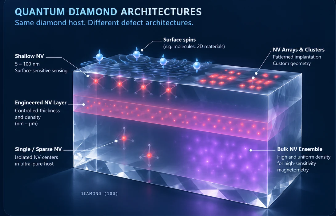
This is why “quantum diamond” covers several distinct material architectures. A low-defect electronic-grade substrate serves a different purpose from a shallow-NV sensing surface, a high-density NV ensemble, an implanted array or an isotope-engineered active layer.
The parameters that actually matter
Host purity and spin environment
Electronic-grade diamond minimizes unwanted nitrogen and background defects. It is the starting point for experiments that require a clean host, controlled implantation or low native NV density.
NV depth and surface engineering
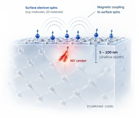
Near-surface sensing requires control of implantation depth and surface condition. Nova supports shallow NV centers in the 5–100 nm range, with 14N or 15N implantation and surface termination options including oxygen- and hydrogen-terminated surfaces.
NV density
Single-defect experiments, patterned arrays and ensemble sensing require different defect densities. NV ensemble material is typically specified by target concentration and active-layer architecture, while arrays and clusters require spatial control in addition to density.
Isotope composition
Reducing the 13C nuclear-spin bath is useful when the experiment benefits from an isotope-controlled host. Nova supports 12C-enriched material above 99.99%, including engineered active layers and controlled 14N or 15N configurations.
Choosing the right quantum diamond
| Material architecture | Typical reason to choose it | Key variables |
|---|---|---|
| Electronic Grade | Clean host for implantation, low-background spin experiments and custom defect creation | N <5 ppb, orientation, thickness, surface finish |
| Shallow NV | Nanoscale sensing close to the diamond surface | Depth, isotope, surface termination, roughness |
| NV Ensemble | High-sensitivity sensing, wide-field imaging and microwave/maser experiments | NV density, layer/bulk architecture, geometry |
| NV Arrays & Clusters | Spatially defined defects and engineered multi-NV structures | Pitch, cluster spacing, dose, depth |
| Isotope-Engineered | Reduced 13C spin bath and isotope-defined structures | 12C enrichment, active-layer thickness, N isotope |
| {111} Diamond | Experiments benefiting from NV-axis alignment with the surface normal | Orientation, electronic grade / NV layer / ensemble |
Quantum diamond applications
Quantum sensing & magnetometry
NV spins can be optically initialized and read out while responding to local magnetic fields. Material selection depends strongly on sensing volume: shallow NV centers suit near-surface nanoscale measurements, while ensembles provide larger numbers of sensing spins for high-sensitivity and wide-field measurements.
Nanoscale NMR & spectroscopy
For nanoscale NMR, the NV-to-sample distance becomes a central material parameter. Shallow depth, surface preparation and coherence therefore need to be considered together rather than independently.
Wide-field magnetic imaging
Wide-field imaging commonly uses an NV-rich sensing layer across a polished surface. Uniformity of the active layer, NV density and optical quality can be as important as the nominal concentration.
Quantum information & spin physics
Low-defect hosts, isotope engineering and spatially controlled NV structures support experiments involving coherent spin control, coupled defects and quantum-register concepts.
Maser & microwave quantum devices
High-density NV ensemble material can be combined with resonant microwave structures and optical pumping. Larger sample dimensions, side polishing, bevels and custom geometry may become part of the material specification.
From material specification to experiment-ready diamond
A useful quantum-diamond specification begins with the experiment, not a catalog number. The target sensing modality or spin experiment determines the host purity, defect architecture, isotope composition, orientation and geometry.
Nova combines CVD/HPHT diamond supply with defect engineering and post-growth processing. Available work includes implantation, controlled NV architectures, laser cutting and micromachining, ultra-precision polishing, orientation cutting, thinning, micro-sample fabrication and custom side-wall geometry.
Frequently asked questions
What is the difference between electronic-grade diamond and NV diamond?
Electronic-grade diamond is optimized for a very low-defect host. NV diamond intentionally contains or receives engineered nitrogen-vacancy centers for spin-based experiments.
How shallow can NV centers be made?
Nova supports shallow NV configurations in the 5–100 nm range. The appropriate depth depends on the sensing target, surface environment and required spin performance.
Can the diamond be isotope engineered?
Yes. 12C-enriched material above 99.99% is available, including controlled active-layer structures and 14N or 15N options.
Why use {111} diamond for NV-center research?
For a {111}-oriented surface, one NV axis can align with the surface normal, which is useful in experiments where crystallographic alignment matters.
Can Nova customize the final diamond geometry?
Yes. Custom size, orientation, thinning, polishing, micro-cubes, bevels and side-wall geometries can be discussed around the experiment.