
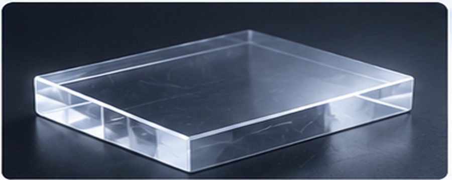
01 · Host Material
Electronic Grade Diamond
High-purity single-crystal diamond for low-background measurements, controlled implantation and single-defect fabrication.
Explore →From ultra-low-background host crystals to engineered NV depth, density, isotope, orientation, form factor and geometry, Nova Crystal builds quantum materials around the parameters that determine the experiment.
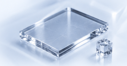
Nova’s primary product platform is quantum-grade diamond. Each product page goes deeper into the relevant purity, NV architecture, isotope, orientation and processing window.
High-purity single-crystal diamond for low-background measurements, controlled implantation and single-defect fabrication.
Explore →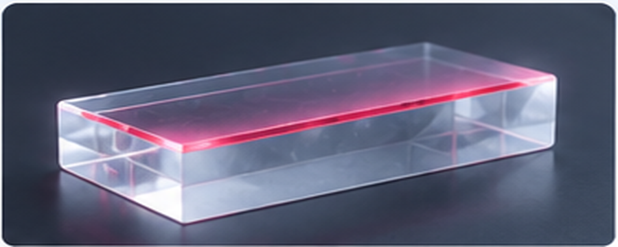
Near-surface NV centers engineered for surface-spin sensing, nanoscale magnetometry and related experiments.
Explore →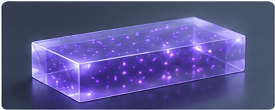
Uniform NV ensemble material and engineered active volumes for magnetometry, wide-field imaging, maser and device integration.
Explore →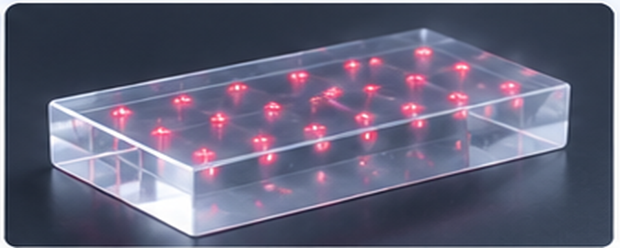
Position-defined single NV, cluster and ensemble-array architectures for scalable sensing and interaction studies.
Explore →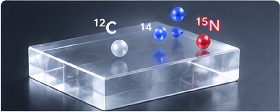
¹²C-enriched material with reduced ¹³C nuclear-spin background plus controlled ¹⁴N / ¹⁵N doping, in bulk or active-layer formats.
Explore →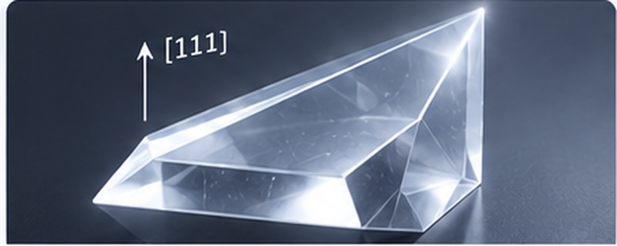
{111}-oriented electronic-grade, shallow-NV and NV-ensemble platforms for experiments where surface-normal NV alignment and field geometry matter.
Explore →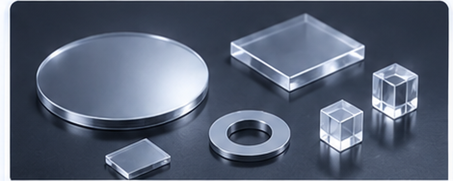
Laser cutting, ultra-precision polishing, orientation cutting, thinning, side polishing, bevels, micro-cubes and experiment-specific geometries.
Explore Processing →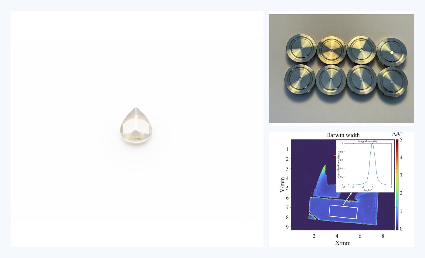
ATR, Raman crystals, optical windows, DAC and precision X-ray optics—with metallization, flange customization, welding and integrated optical assembly available.
Explore →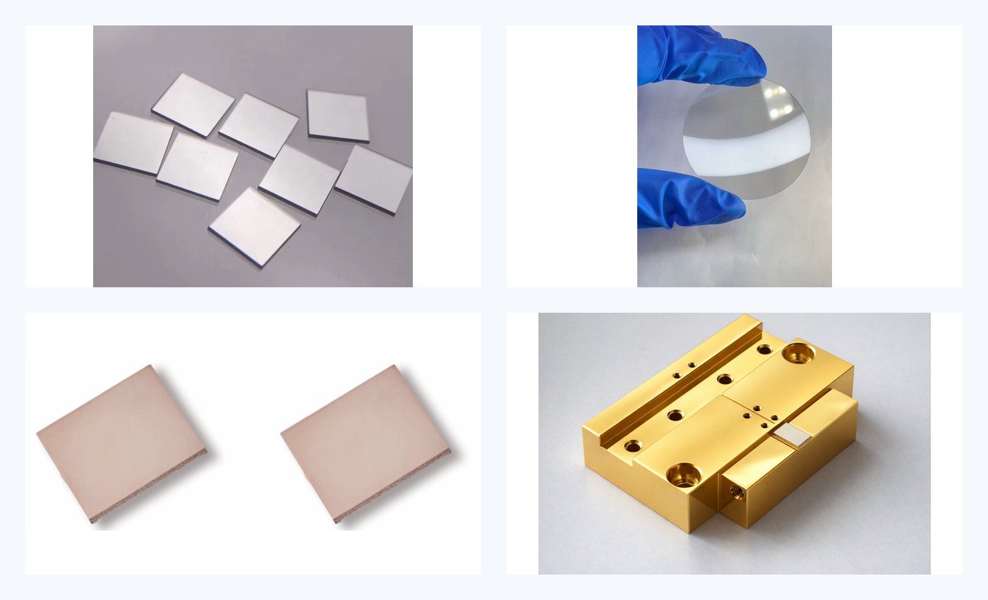
Single-crystal, polycrystalline, diamond–copper and ultra-thin diamond formats—with metallization, bonding and integrated thermal-module support.
Explore →Beyond NV diamond, Nova Crystal supports selected emerging quantum-material platforms for spin, photonics, sensing and hybrid-device research. Current capabilities include SiV centers in diamond, defect centers in SiC, quantum emitters in hBN and graphene-based structures, with project-specific support spanning materials, ion implantation, annealing, processing and characterization.
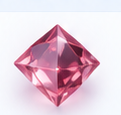
Silicon-vacancy color centers for optical quantum emitter and photonics research.
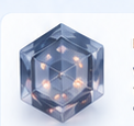
Wide-bandgap defect platforms for spin, sensing and quantum-device research.
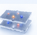
Two-dimensional emitter systems for nanoscale optics and quantum photonics research.
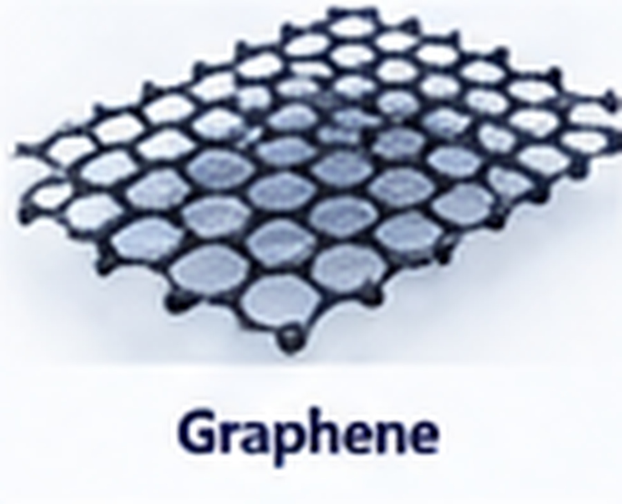
Graphene-based structures for 2D quantum-material, defect and hybrid-device research.
Send the host material, target defect, concentration, isotope, orientation, dimensions, thickness, surface finish and application. We can discuss the configuration around the experiment rather than force it into a fixed catalog SKU.
For detailed product brochures, complete specifications and available product-parameter characterization or test data, please contact Nova Crystal by email.
Nova Crystal provides advanced diamond materials across three main application areas: quantum diamond for NV-center research and sensing, optical diamond for spectroscopy, laser, DAC and X-ray systems, and thermal-management diamond for high-heat-flux electronics and device integration. Custom processing, metallization, bonding, welding and component integration are available by project.
Product options include electronic-grade CVD diamond, shallow NV diamond, NV ensemble and patterned NV arrays, isotope-engineered diamond, {111} diamond, diamond ATR crystals, Raman diamond, optical windows, X-ray monochromators, single-crystal and polycrystalline heat spreaders, diamond-copper structures and transferable ultra-thin diamond films.