{111}
Diamond
(111)-oriented single-crystal diamond for experiments where NV-axis alignment, magnetic-field geometry and surface crystallography matter.
![(111)-oriented diamond with an NV axis aligned to the [111] surface normal and magnetic field parallel to the NV axis](assets/111-hero.jpg)
Make the crystal geometry
work with the spin axis.
On a (111) surface, one NV orientation is parallel to the [111] surface normal. For experiments using that NV family, the magnetic field can be applied along the surface normal and directly along the NV axis.
Surface normal, NV axis and magnetic field on one line.
Simpler magnetic-field alignment
For the [111]-aligned NV orientation, B can be applied normal to the surface rather than at an oblique angle.
Useful near-surface geometry
A surface-normal NV axis is convenient for shallow-NV sensing, scanning geometries and surface-sensitive measurements.
Clear experimental axis
Surface, optical axis and spin quantization geometry can be designed around the same crystallographic direction.
Electronic-grade or NV engineered
Use a high-purity {111} host, or combine {111} orientation with custom NV depth, density and isotope engineering.
Choose the {111} platform
around the experiment.
{111} diamond is available as electronic-grade host material, an NV-active layer on a {111} host, or uniform NV-ensemble material. Thickness, polishing and custom geometry remain processing options across all three platforms.
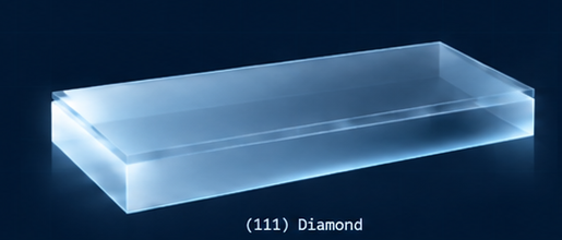
{111} Electronic Grade
High-purity single-crystal diamond with N < 5 ppb available for low-background measurements, single-NV fabrication and controlled implantation.
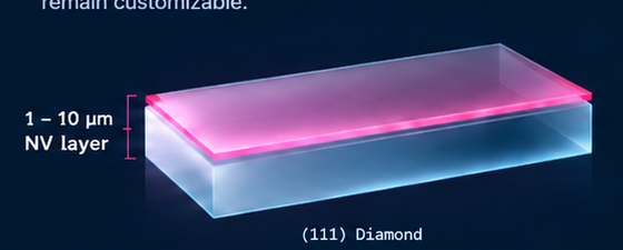
{111} Single & NV Layer
An NV-active layer is engineered directly beneath the {111} surface. Typical active-layer thickness is 1–10 μm, with NV density and layer design customizable around the experiment.
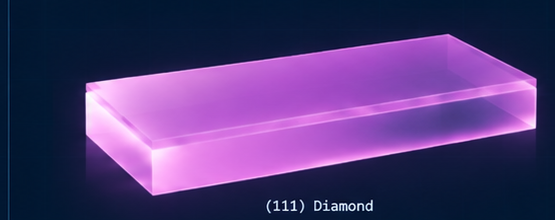
{111} NV Ensemble
Uniform NV-ensemble material across the {111} crystal volume for magnetometry, wide-field imaging, maser and device-oriented sensing. Bulk concentration is customized by project.
Define the orientation,
then define the surface.
Final specifications depend on growth route, thickness, cutting geometry and downstream NV or device requirements.
Where {111} orientation
changes the experiment.
The main value of {111} is geometric: the crystal surface can be chosen to simplify the relationship between the sample, the NV axis and the external field.
NV Magnetometry
Surface-normal field geometry for selected NV orientations in precision magnetic sensing.
NV Layer Sensing
{111}-aligned NV layers can be engineered for surface-sensitive sensing, wide-field measurements and custom device geometries.
NV Arrays & Devices
Combine {111} substrates with patterned implantation, arrays and custom quantum structures.
Quantum Photonics
Orientation-controlled single crystal for optical structures, emitters and integrated device research.
From crystal orientation
to experiment-ready geometry.
Nova can combine orientation cutting with thickness control, polishing, NV engineering and surface chemistry according to the final setup.
Need a {111} diamond built around your field geometry?
Send the target orientation, dimensions, thickness, NV architecture and surface requirements. We can translate them into a material and processing specification.