Start with Nova’s in-depth technical guides, then explore focused material topics, ongoing project updates and direct access to brochures, specifications and available characterization data.
Our primary long-form resource for understanding quantum diamond, NV-center material architectures and how experimental requirements translate into material specifications.
Materials, Engineering and Applications — a practical guide to electronic-grade diamond, shallow NV centers, NV ensembles, arrays, isotope engineering, {111} diamond and experimental material selection.
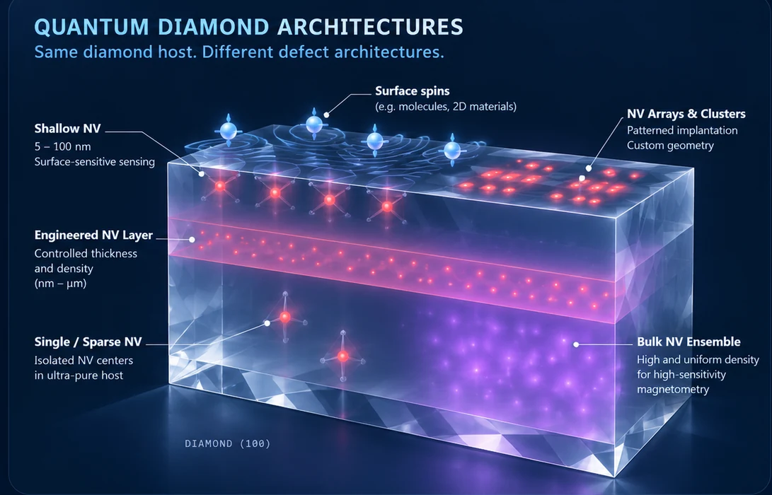
Focused entry points for the material systems and engineering capabilities most relevant to Nova’s current work.
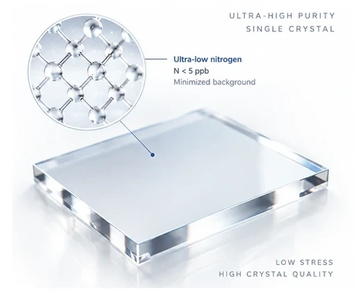
Host purity, shallow NV, ensembles, arrays, isotope engineering and orientation.
MPCVD growth, nitrogen incorporation, ion implantation, annealing and controlled defect structures.
ATR, Raman crystals, optical windows, DAC components, X-ray monochromators and integration.
Single-crystal and polycrystalline heat spreaders, diamond-copper and transferable ultra-thin films.
Real material cases, experimental visuals and ongoing technical notes are published through LinkedIn as the work develops.
First-hand material cases, CVD growth, processing, polishing and integration work from Nova Crystal.
Nova Crystal on LinkedIn →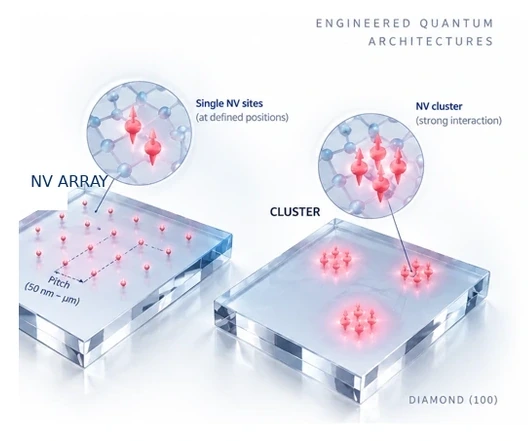
NV-center materials, quantum sensing, sample architecture and application-oriented technical discussions.
Ray Song on LinkedIn →For product brochures, complete specifications, available characterization/test data and experiment-specific discussion, contact Nova directly.
Company updates, real samples, processing cases and application examples.
Follow Nova Crystal →Send your target experiment, material architecture and key parameters. We can provide available technical information and discuss a suitable specification.
nova@novacrystal.hk →