Shallow NV
Diamond
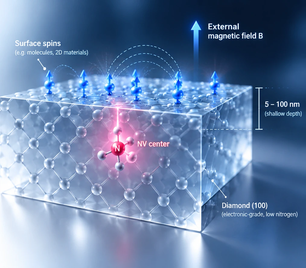
Near-surface NV centers engineered within 5–100 nm of the diamond surface for strong coupling to external spins, nanoscale magnetic sensing and surface-sensitive NMR.
Bring the NV sensor
closer to the signal.
For surface-sensitive experiments, NV depth directly affects coupling to spins and fields outside the diamond. The objective is not simply “as shallow as possible”, but the right depth with usable spin performance and a controlled surface.
Depth sets the sensing distance.
Near-surface NV centers can interact with magnetic moments and spin ensembles outside the diamond, making them suitable for nanoscale sensing and surface-sensitive spectroscopy.
surface quality + spin coherence still matter
5–100 nm is a platform,
not one fixed recipe.
Implantation species, energy, dose, crystal orientation, annealing and surface preparation are selected around the target NV architecture.
Depth is only one variable.
The shallow-NV architecture is defined together with the host crystal and surface.
Configure the shallow-NV layer.
These values define the normal engineering window. Final implantation and processing parameters should be selected around the measurement requirement.
The surface is part
of the quantum device.
When the NV center is only nanometers below the surface, surface chemistry can influence charge stability, noise and device integration. Nova can prepare H- or O-terminated surfaces according to project requirements.
Hydrogen-Terminated Surface
Available for experiments or device structures where hydrogen surface chemistry is required. Surface preparation is coordinated with the NV depth and downstream device process.
Oxygen-Terminated Surface
Available for near-surface sensing workflows requiring an oxygen-terminated interface, with polishing and cleaning coordinated to the final surface condition.
Built for surface-sensitive
quantum measurements.
Shallow NV centers are most useful when the signal source sits outside or immediately above the diamond surface.
Nanoscale Magnetic Sensing
Detect localized magnetic fields and magnetic textures with a near-surface spin sensor.
Nanoscale NMR / MRI
Surface-sensitive detection of nuclear spins in small sample volumes and molecular systems.
Scanning NV Probes
Shallow NV architectures for high-spatial-resolution scanning quantum sensing platforms.
Surface & 2D Materials
Study magnetic and spin phenomena in thin films, interfaces and two-dimensional materials.
Specify the sensing problem,
then engineer the diamond.
Nova supports the workflow from substrate selection through implantation, NV formation, surface preparation and characterization.
Tell us the sensing depth you need.
Send the target depth, orientation, isotope, dose or application. We can translate it into a shallow-NV material specification.