01 · QUANTUM SENSING
Quantum Sensing & Magnetometry
Diamond spin sensors for DC/AC magnetic-field measurements, scanning-probe experiments and precision sensing.
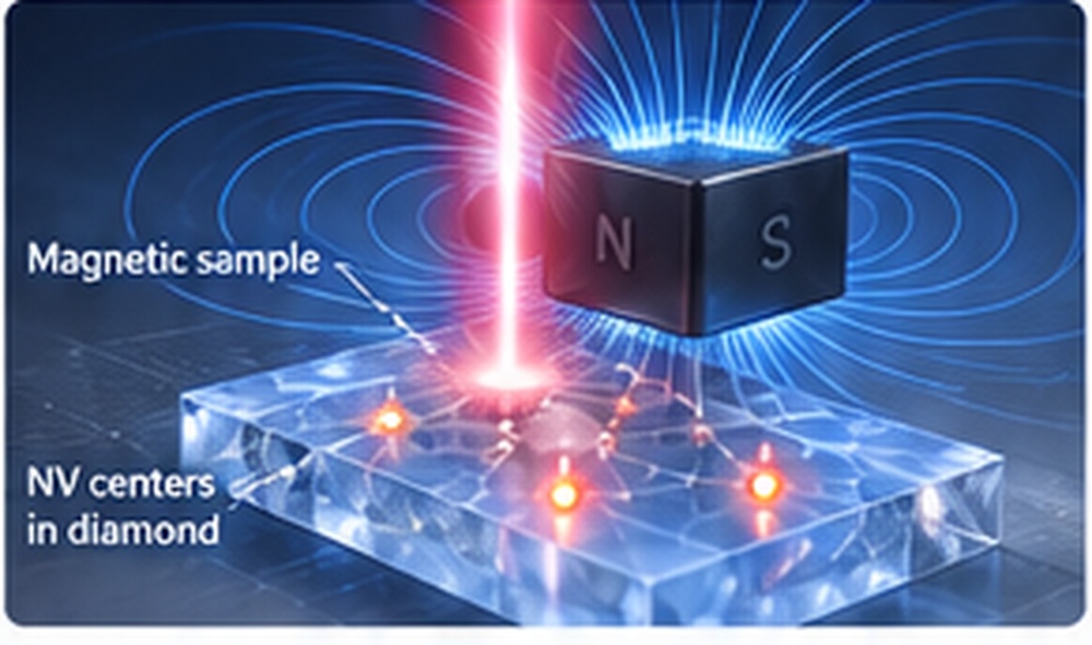
Choose the diamond platform around what you need to measure, image or build—from near-surface spin sensing and nanoscale NMR to wide-field magnetic imaging, coupled NV systems and quantum devices.
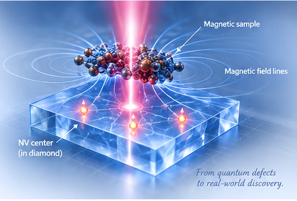
Each application maps to a different combination of NV depth, density, crystal orientation, isotope composition and sample geometry.
Diamond spin sensors for DC/AC magnetic-field measurements, scanning-probe experiments and precision sensing.
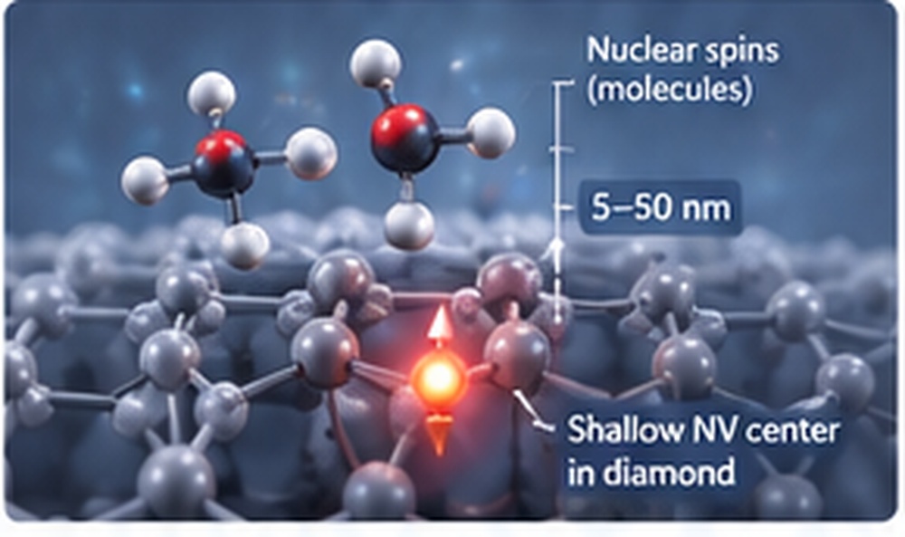
Near-surface NV centers engineered close to the diamond surface for stronger coupling to external nuclear and electronic spins, supporting nanoscale NMR and surface-sensitive spectroscopy.
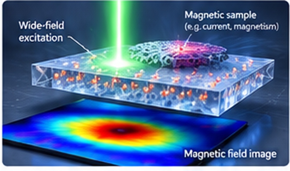
NV-ensemble and engineered NV-layer materials for spatially resolved magnetic-field and current-density imaging.
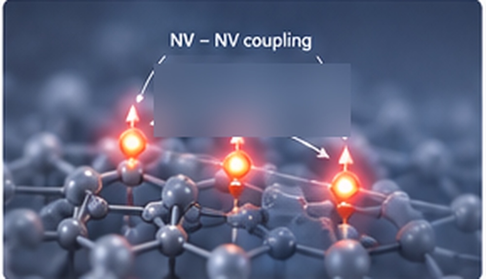
Single NVs, patterned arrays and compact NV clusters for addressable spins, NV–NV coupling and multi-spin studies. Inter-NV distance can be engineered around approximately 20–500 nm for cluster-oriented experiments.
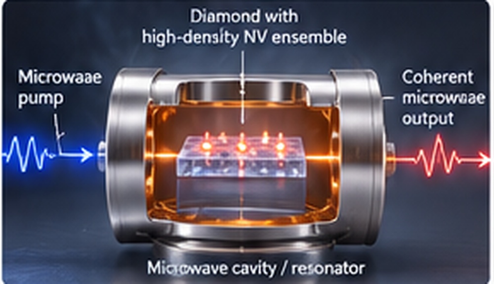
Engineered NV-ensemble materials for experiments involving spin polarization, microwave interaction and maser-oriented architectures.
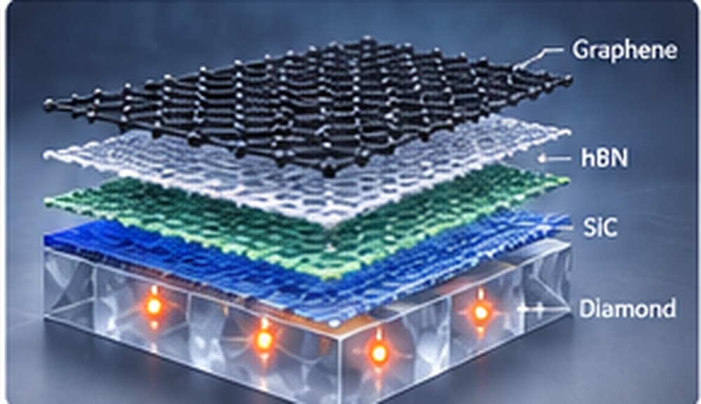
Custom diamond geometry and research-driven integration with SiC, hBN, graphene and other emerging quantum-material systems.
Magnetic field, external spins, spatial imaging, coupled spins or device operation.
Single, shallow, ensemble, engineered layer, patterned array or cluster.
Purity, isotope, {100}/{110}/{111} orientation, depth and NV concentration.
Bulk, thin plate, small sample, cutting, polishing and custom processing.
Tell us the target measurement, approximate NV depth or density, orientation and sample geometry. We can help map the experiment to a suitable material configuration.
For detailed product brochures, full specifications and available characterization or parameter-test data, please contact Nova Crystal by email.