Select the quantum function of each layer
Diamond can provide engineered NV centers, while SiC, hBN, graphene or other materials can support complementary optical, electronic or defect-related functions.
Nova supports research that combines diamond with SiC, hBN, graphene and other quantum-material platforms. Material selection, defect engineering, precision processing and device geometry can be coordinated around the final photonic, microwave, electronic or hybrid architecture.
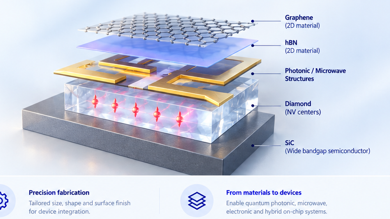
Diamond, SiC, hBN, graphene and related quantum materials can be considered within one device concept.
Cutting, polishing, thinning, custom geometry and other post-growth processing can be matched to integration requirements.
Material engineering can be coordinated with implantation, processing, characterization and collaborative device development.
Hybrid quantum devices depend on more than choosing the right substrate. Surface quality, layer placement, optical access, electrode geometry, crystal orientation and mechanical tolerance can all determine whether the integrated system works as intended.
Diamond can provide engineered NV centers, while SiC, hBN, graphene or other materials can support complementary optical, electronic or defect-related functions.
Implantation, annealing, surface preparation and characterization can be incorporated when the device requires controlled defects or engineered interfaces.
Thickness, small-sample fabrication, side polishing, custom shapes, orientation control and precision processing can be matched to the photonic or microwave architecture.
Nova’s core strength remains quantum diamond, while SiC, hBN, graphene and other emerging systems are supported as custom or collaborative research platforms.
Ultra-low-nitrogen single-crystal diamond for controlled defect engineering and low-background quantum devices.
View Electronic Grade →Shallow NV, NV ensemble, array and cluster architectures for integrated spin, sensing and quantum-device experiments.
View NV Platforms →¹²C-enriched material and controlled nitrogen isotopes for experiments where the surrounding nuclear-spin environment is important.
View Isotope Engineering →Selected custom and collaborative projects involving SiC defect systems, hBN emitters, graphene and other emerging quantum materials.
Explore Emerging Materials →For product brochures, complete specifications and available characterization or parameter-test data for quantum diamond and emerging material platforms, please contact Nova Crystal by email.