Nova Crystal Technologies LimitedNOVA CRYSTALTECHNOLOGIES LIMITED
QD · Custom Quantum Diamond

Build the diamond
around the experiment.

Custom quantum diamond coordinates host purity, NV architecture, isotope composition, crystal orientation, geometry, surface chemistry and characterization as one material specification.

Depth · Density · Pattern¹²C · ¹⁴N · ¹⁵N{100}/{110}/{111}Ra < 1 nmH / O termination
Material firstStart from host purity and crystal quality.
Defect architectureCoordinate depth, density and spatial structure.
Geometry mattersSize, thickness, side faces and orientation can be engineered.
Surface is part of the specPolishing and H/O termination for near-surface work.
Engineering Variables

Customize the variables that
change the experiment.

Custom quantum diamond is most useful when several parameters must be coordinated at the same time—for example shallow depth with a low-background host, a specific isotope, a {111} surface and defined surface chemistry.

Engineering logic

Do not optimize one parameter in isolation.

Depth, density, isotope composition, strain, orientation, geometry and surface condition can all influence the final measurement. The material should be designed as a system.

Host → Defect → SurfaceResearch-ready
01 · HOST

Purity & Growth

Electronic-grade CVD or HPHT starting material with low unwanted nitrogen and defect background.

N < 5 ppb · CVD / HPHT
02 · DEFECT

NV Architecture

Single, shallow, ensemble, patterned array or compact cluster structures according to the experiment.

5–100 nm shallow · 5–70 nm array
03 · ISOTOPE

Isotope Engineering

¹²C enrichment and controlled ¹⁴N / ¹⁵N incorporation for coherence-sensitive or isotope-defined structures.

¹²C > 99.99% · ¹⁴N / ¹⁵N
04 · GEOMETRY

Crystal & Device Geometry

Orientation, lateral size, thickness, chamfer/bevel, sidewall angle and side polishing can be project-specific.

{100}/{110}/{111} · custom geometry
05 · SURFACE

Surface Engineering

Ultra-fine polishing, cleaning and hydrogen or oxygen termination for optical, sensing and device requirements.

Ra < 1 nm · H / O termination
06 · VERIFY

Characterization

Requested material and spin characterization can be coordinated with the project specification.

PL · NV density · T₂ · T₂* · T₁
Precision Processing

From crystal to custom geometry.

Complete post-growth processing for experiment-ready diamond components—from laser cutting and ultra-precision polishing to orientation control, thinning and micro-scale sample preparation.

Flexible geometry. Controlled surfaces.

Nova supports custom size, shape, orientation and surface preparation while maintaining material quality and tight dimensional control.

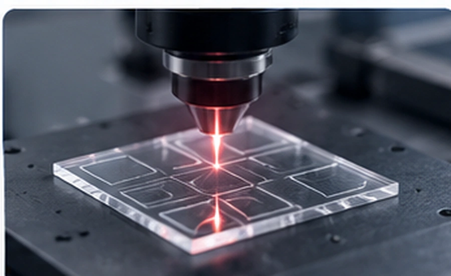
01 · LASER PROCESSING

Laser Cutting & Micromachining

Precision cutting for thin plates, membranes, micro-cubes and custom outlines, including subdivision of larger crystals into multiple research samples.

Laser cutting and micromachining of diamond samples
Minimum feature size~50 μm
Edge qualityClean / low damage
GeometryCustom 2D / 3D
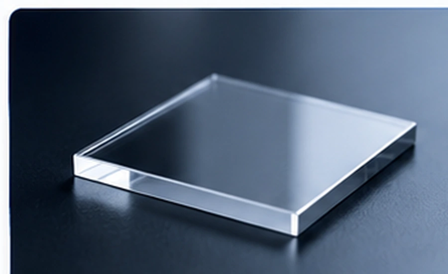
02 · SURFACE FINISH

Ultra-Precision Polishing

Top, bottom and side polishing for optical- and quantum-grade surfaces. Side faces can also be polished for resonator, maser and device-integration geometries.

Ultra-precision polished diamond plate
Surface roughnessRa < 1 nm
FacesTop / bottom / side
UseOptical / quantum
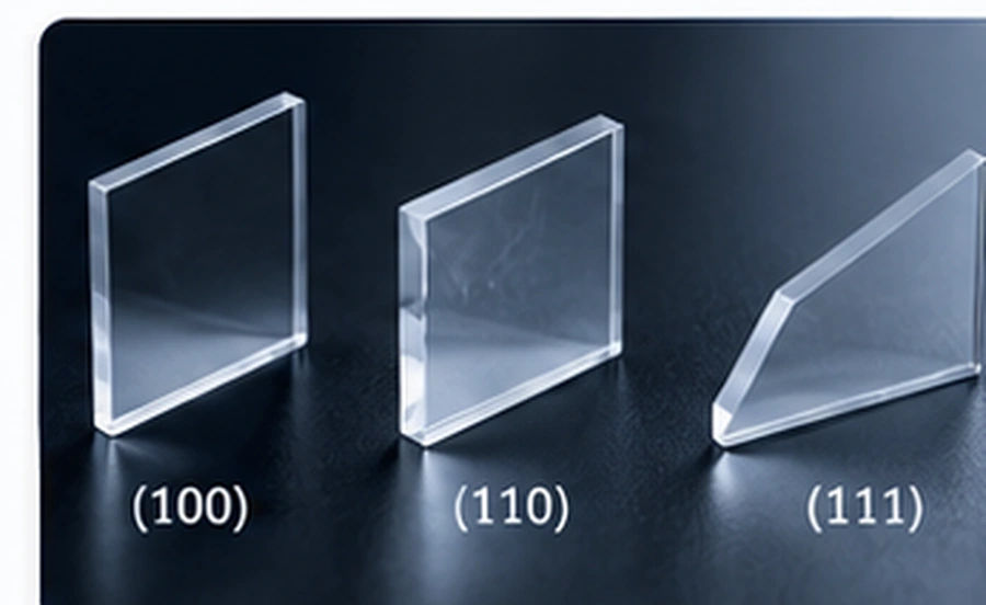
03 · ORIENTATION

Orientation Cutting & Thinning

Controlled cutting to obtain {100}, {110}, {111} and other orientations, followed by thinning, dimensional finishing, chamfer, bevel and sidewall-angle control.

Complete {100}, {110} and {111} diamond orientation samples
Orientations{100} / {110} / {111}
Thickness50 μm → several mm
Angular deviation≤ 1°
Dimensional tolerance±0.05 mm
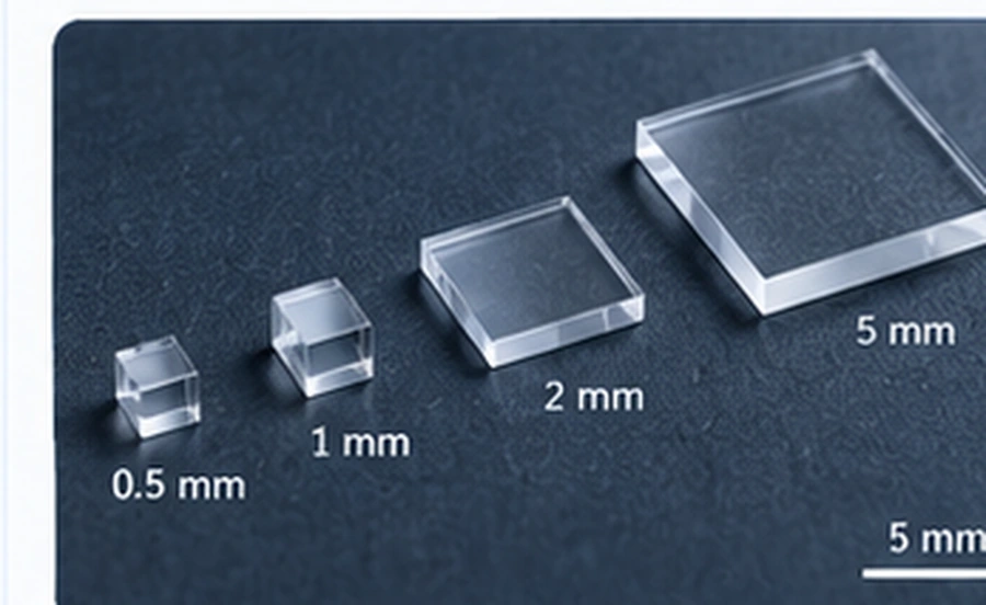
04 · SMALL SAMPLES

Small Samples & Micro-Cubes

Fabrication of compact samples for quantum optics, micro-resonators, hybrid systems and method development, including sub-millimeter cubes, thin plates and custom geometries.

Complete set of small diamond samples and micro-cubes
Minimum length0.2 mm
Minimum thickness0.05 mm
FormatsCubes / plates / membranes
Typical Custom Configurations

Different experiments need
different material architectures.

These are representative starting configurations. Final ranges and deliverables are confirmed project by project.

01 · SURFACE SENSING

Shallow NV

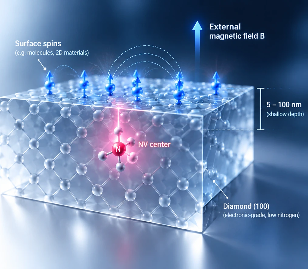
Shallow NV centers near a diamond surface

Low-background host, engineered near-surface NV depth and surface preparation for nanoscale sensing or NMR.

5–100 nm · H/O
02 · PATTERNED DEFECTS

Array / Cluster

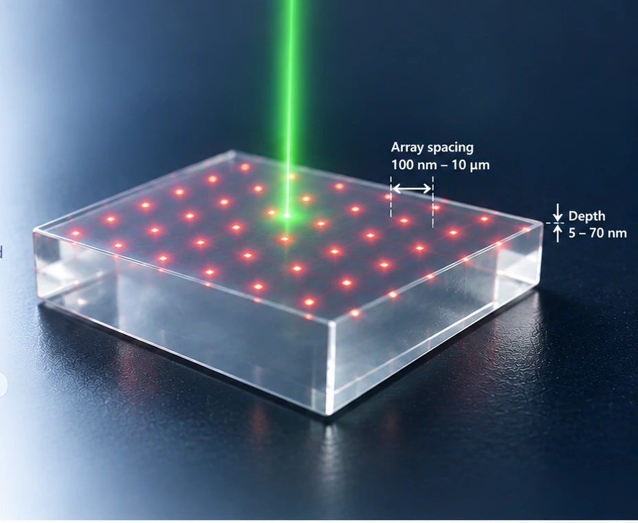
Patterned NV array in diamond

Position-defined NV sites, custom spatial pattern, ensemble pixels or compact NV clusters for interaction studies.

5–70 nm · cluster 20–500 nm
03 · COHERENCE

Isotope Layer

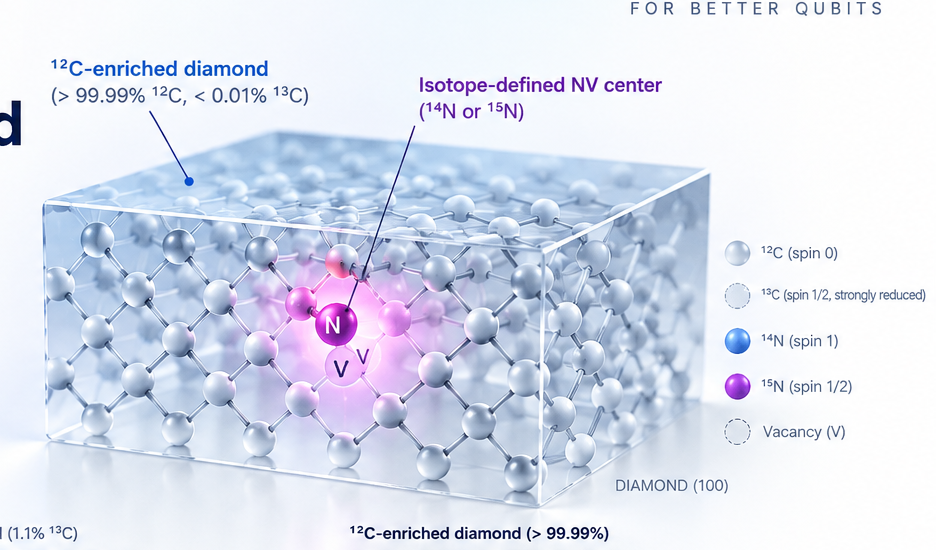
Isotope-engineered diamond lattice

¹²C-enriched material with engineered ¹⁴N / ¹⁵N incorporation and a custom active layer.

¹²C > 99.99% · 1–20 μm
04 · DEVICE / MASER

Bulk Ensemble

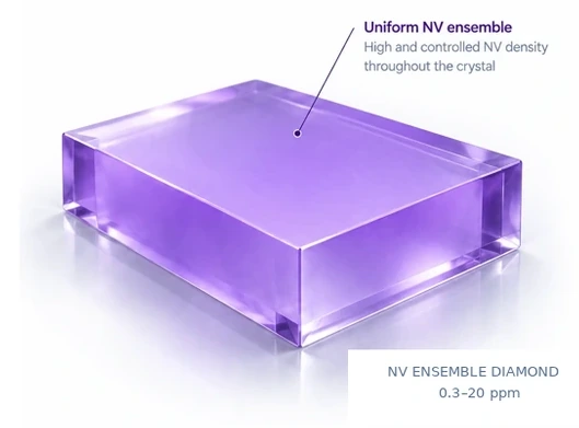
Uniform NV ensemble diamond

Uniform high-density ensemble material with custom size, thickness, side geometry and polished faces for device integration.

0.3–20 ppm · up to ~10 mm typical
05 · ALIGNMENT

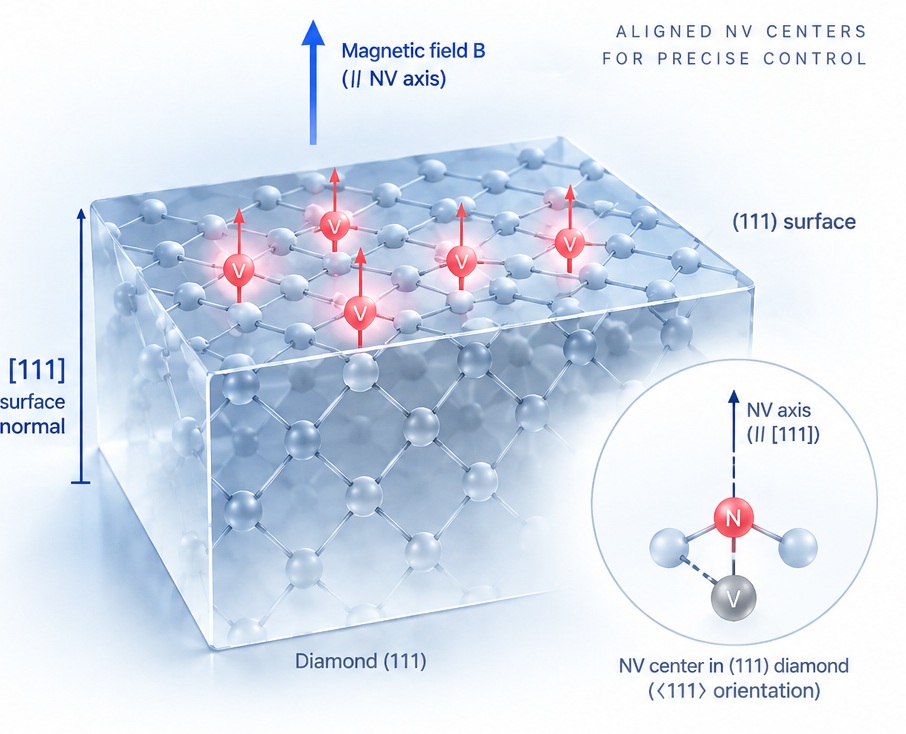
{111} Platform

Diamond 111 NV alignment and magnetic field geometry

{111}-oriented host, NV layer or ensemble when surface-normal NV alignment and magnetic-field geometry are important.

{111} · custom NV architecture
Project Workflow

From measurement requirement
to finished material.

A custom project starts with the experimental constraint. Nova then translates it into a coordinated host, NV, isotope, geometry, surface and verification plan.

Requirement-drivenIterative R&D supported
01
Define the experimentTarget signal, sensing distance, optical/microwave geometry, sample environment and integration limits.
INPUT
02
Select the hostGrowth method, purity, isotope composition and crystallographic orientation.
HOST
03
Design the NV architectureSingle, shallow, ensemble, array, cluster or engineered active layer.
NV
04
Define geometry & surfaceSize, thickness, cutting, bevel, side polishing, Ra target and H/O termination.
FORM
05
Process & activateImplantation or growth-based defect engineering, annealing and NV formation.
BUILD
06
Characterize & deliverRequested material, optical and spin characterization according to the project.
VERIFY
Custom Specification Window

A specification can combine
multiple engineering dimensions.

The values below are representative capabilities and product families already used across Nova's quantum-diamond platform. Final feasibility depends on the combined configuration.

Host material
Electronic-grade CVD / HPHT single-crystal diamond
Nitrogen background
N < 5 ppb for electronic-grade host configurations
Crystal orientation
{100} / {110} / {111}; orientation processing by project
Shallow NV depth
5–100 nm typical custom window
NV array depth
5–70 nm; custom spatial pattern
Cluster inter-NV distance
20–500 nm target range
NV concentration
Single / sparse → 0.3–20 ppm ensemble range; project-specific
Isotope engineering
¹²C > 99.99%; controlled ¹⁴N / ¹⁵N options
Isotope / NV active layer
1–20 μm custom layer configurations
Typical lateral size
2–10 mm classes; larger or non-standard geometry by project
Thickness / geometry
Thin plates to ~3 mm-class bulk structures; chamfer, bevel, sidewall angle and side polishing by project
Precision processing
Laser cutting, micromachining, orientation cutting, thinning, micro-cubes and small custom samples
Processing tolerance
Angular deviation ≤ 1°; dimensional tolerance ±0.05 mm typical; min length 0.2 mm; min thickness 0.05 mm
Surface
Ra < 1 nm typical polished target; H / O termination available
Characterization
PL / NV density / T₂ / T₂* / T₁ / surface or other agreed project checks
Custom projects may require experimental iteration. Combined specifications are reviewed for compatibility before quotation and scheduling.
Applications

Custom material for experiments
that do not fit a standard part.

Custom engineering is especially useful when quantum performance depends on several coupled material parameters.

01

Nanoscale NMR

Coordinate shallow depth, host purity and surface chemistry around near-field coupling.

02

Wide-Field Sensing

Engineer uniform ensemble density, active volume and optical geometry for imaging.

03

Quantum Maser

Coordinate ensemble concentration with crystal size, thickness, side angle and polished faces.

04

Quantum Information

Patterned single NVs, clusters, isotope control and orientation for spin-based experiments.

05

Device Integration

Custom geometry, thin structures, polishing and surface preparation for hybrid devices.

Have a non-standard quantum diamond requirement?

Send the target experiment, required NV architecture, size, orientation, depth/density, isotope requirement and any surface or geometry constraints. We can translate it into a technical specification.

Discuss a Custom Project →