Electronic Grade
Diamond
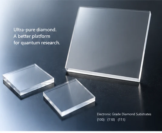
Ultra-high-purity, low-stress single-crystal diamond engineered as a clean host for single-NV research, controlled defect creation and quantum-device fabrication.
A cleaner host gives you
more control over the defect.
Electronic-grade diamond minimizes unwanted nitrogen and native NV background before implantation, irradiation or other defect-engineering steps.
Start from the diamond, not from the background.
For single-NV experiments and engineered defects, the host crystal should contribute as little unwanted spin and optical background as possible.
Suitable as a starting substrate for controlled NV creation and low-background quantum measurements.
Helps distinguish deliberately engineered defects from pre-existing NV centers.
Prepared for implantation, lithography, surface engineering and optical experiments.
Select crystallographic orientation around NV alignment, optical geometry and device design.
The starting material for
NV engineering.
Electronic-grade diamond is not the end architecture. It is the controlled host on which shallow NV, arrays, isotope-defined layers and other quantum structures can be built.
Single-NV Research
Low-background host material for locating and studying isolated color centers.
Ion Implantation
Clean starting substrate for controlled ¹⁴N/¹⁵N implantation, depth engineering and patterned defect creation.
Quantum Devices
Precision-polished diamond for photonics, sensing structures and heterogeneous device integration.
Configure the host crystal.
Standard electronic-grade material is available in multiple orientations and dimensions, with custom processing according to the experiment.
A high-purity foundation
for quantum experiments.
Use electronic-grade diamond when the experiment requires a controlled host before defect creation or device fabrication.
Single-NV Studies
Low-background material for isolated color-center spectroscopy and spin experiments.
Controlled Implantation
Starting substrate for shallow NV, ¹⁴N/¹⁵N implantation, arrays and clusters.
Quantum Photonics
High-quality single crystal for optical structures, waveguides and photonic-device research.
Device Integration
Precision-polished diamond for sensing chips, hybrid structures and downstream fabrication.
Start with the host,
then build the architecture.
Nova can combine electronic-grade substrates with orientation control, precision polishing, implantation, NV formation and surface preparation.
Need a specific electronic-grade substrate?
Send the required size, thickness, orientation, surface finish and downstream experiment. We can translate it into a material specification.