
NV Array
Diamond
Spatially defined NV architectures created by patterned implantation for controlled positioning, custom pitch and scalable quantum-device research.
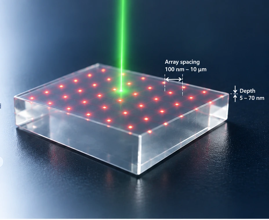
Control where the NVs are,
not only how many.
NV arrays add a spatial-design variable to quantum diamond. The same electronic-grade host can be patterned as isolated sites, repeated arrays or localized clusters depending on the measurement and interaction length scale.
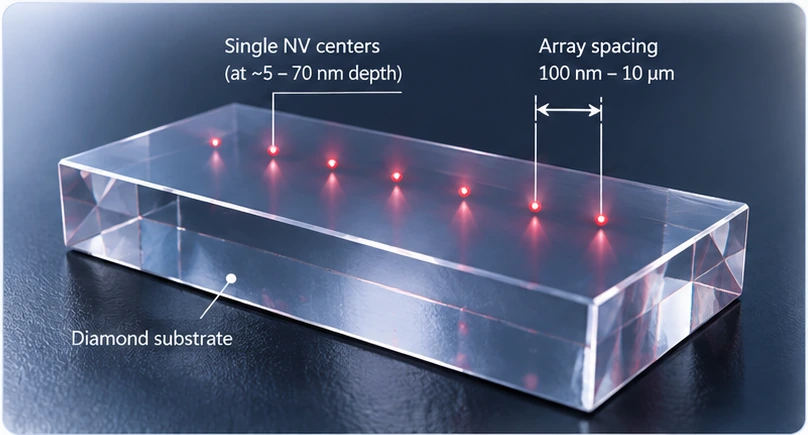
Single-NV / sparse arrays
Patterned implantation is used to create spatially defined sites intended for isolated or sparse NV formation, useful for single-defect studies, quantum registers and position-controlled sensing.
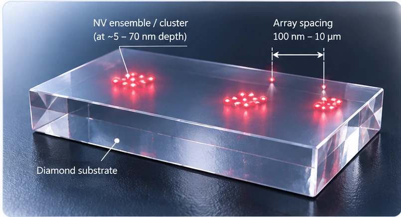
Ensemble arrays & clusters
Higher-dose patterned regions create local NV ensembles or compact clusters, enabling scalable sensor pixels, strong local fluorescence and experiments that depend on NV–NV proximity.
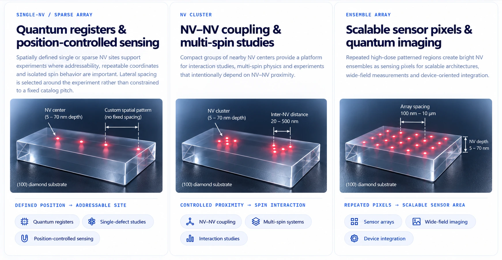
Different NV architectures
enable different experiments.
Patterned implantation is valuable because the spatial architecture itself becomes an experimental parameter. Sparse sites, compact clusters and repeated ensemble pixels address different sensing, interaction and scaling requirements.
Pattern, depth and density
are designed together.
The final NV architecture depends on mask geometry, implantation species, energy, dose, host material, annealing and surface preparation. Nova can define these variables around the target experiment.
Geometry
Square, linear, grid, local cluster or custom patterns can be designed around optical and device geometry.
Implant Energy
2–50 keV implantation supports typical NV depths of 5–70 nm, including commonly used 5, 10, 20, 30 and 70 nm targets; project-specific conditions are available.
Ion Selection
¹⁴N⁺ and ¹⁵N⁺ are available for NV engineering; selected Si implantation projects can also be discussed.
Finish & Termination
Ultra-fine polishing plus hydrogen or oxygen termination can be selected around shallow-array experiments.
Build the array around the experiment.
Parameters below describe the current engineering window. Exact implantation recipe, pitch, dose and expected NV occupancy are confirmed project-by-project because they are coupled to the lithography design and target application.
From array design to
engineered NV architecture.
The workflow can start from a target pitch and sensing geometry rather than a fixed catalog recipe.
Spatial control opens
new experimental geometries.
NV arrays are useful where location, repetition, local density or interaction distance matters as much as the host crystal itself.
Quantum Information
Position-controlled single-NV sites and compact clusters for quantum-register and spin-network studies.
Nanoscale Sensing
Patterned shallow NV sites for local magnetic and electric-field measurements.
Super-Resolution Imaging
Defined NV patterns as test structures for optical localization, confocal and super-resolution methods.
Scalable Sensor Pixels
Large-area patterned ensemble arrays for repeatable sensing regions and device integration.
Need a custom NV array?
Send the target array pitch, active area, desired NV depth, single-site or ensemble architecture, substrate orientation and any surface/characterization requirements. We can translate them into an engineering specification.